
Project: Gate Driver Optimization
Design Specifications:
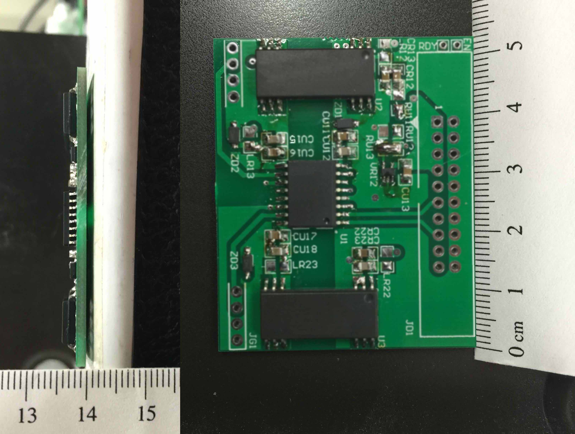
Input: 13.5Vdc~16.5Vdc for power supply and PWM with frequency up to several MHz
Driving ability: 4A peak output current
Highlights: Easily plug, high driving ability with 1.5kVdc peak driver-to-driver differential voltage, compact size(LxWxH: 53mm x 42mm x 4mm)
Application: Isolated gate driver, half bridge, full bridge.
Driving circuit for power switch is very important to Switching-Mode Power Supply (SMPS), as it determines the performance of the power switch. When I’m working on research projects, I find we need to spend lots of time on designing and tuning gate drivers ( Most of our projects are using MOSFETs as the power switch). And in the following test of the power system, it will also take us a lot of time to solder and desolder gate driver circuit or components when the switching channel is failed. So I designed this easily plug isolation gate driver. It can support two isolated output channel (1.5kVdc) with 4A output current at each channel. The thickness including PCB is less than 4mm and it makes the designing of whole power system very convenient.
Links to [Other Projects].